
Which Milestones Would Show Progress in VIS-NIR Integrated Photonics?
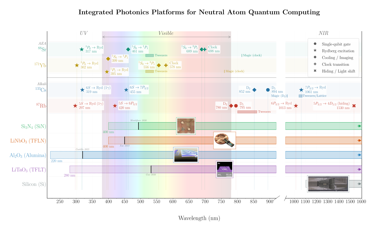
Part 135 of the Neutral Atom Quantum Computation series, covering 3.2.1 VIS-NIR Integrated photonic platforms and the roadmap's guidance on visible and near-infrared integrated photonics.
⚡ Quantum Brief
The milestone is a packaged photonic subsystem that controls real atoms across required wavelengths with lower size and calibration overhead. The evidence should be repeatable and measured inside a representative system rather than inferred from one favorable component result.
Key takeaways
- Integrated photonics can route, split, modulate, stabilize, and emit the many visible and near-infrared wavelengths needed by neutral atom processors.
- Chip-scale photonics may replace bulky optical benches and make thousands of stable control channels manufacturable.
- Short wavelengths increase scattering and fabrication sensitivity, while no single material offers ideal loss, power handling, and modulation everywhere.
- Co-design silicon nitride, thin-film lithium niobate, alumina, tantalate, and hybrid platforms around atomic transitions.
- Measure propagation loss, coupling efficiency, optical power handling, wavelength coverage, phase noise, footprint, yield, and packaging stability. The milestone is a packaged photonic subsystem that controls real atoms across required wavelengths with lower size and calibration overhead.
On this page
Short answerWhy it mattersChallenges and constraintsResearch directionsMetrics and milestonesFrequently asked questionsShort answer
Integrated photonics can route, split, modulate, stabilize, and emit the many visible and near-infrared wavelengths needed by neutral atom processors.
Why it matters
Chip-scale photonics may replace bulky optical benches and make thousands of stable control channels manufacturable.
Challenges and constraints
Short wavelengths increase scattering and fabrication sensitivity, while no single material offers ideal loss, power handling, and modulation everywhere.
Research directions
Co-design silicon nitride, thin-film lithium niobate, alumina, tantalate, and hybrid platforms around atomic transitions.
- 1
Integrate the stack
Evaluate the proposal with the control, compilation, and fault-tolerance assumptions needed by a complete processor.
- 2
Measure representative workloads
Prefer repeated circuit and logical-operation evidence over isolated best-case component measurements.
- 3
Make assumptions explicit
Report scale, error model, calibration, classical support, and resource-accounting boundaries.
Metrics and milestones
Measure propagation loss, coupling efficiency, optical power handling, wavelength coverage, phase noise, footprint, yield, and packaging stability.
The milestone is a packaged photonic subsystem that controls real atoms across required wavelengths with lower size and calibration overhead.
| Dimension | What to report | Why it matters |
|---|---|---|
| Component performance | Measure propagation loss, coupling efficiency, optical power handling, wavelength coverage, phase noise, footprint, yield, and packaging stability. | Shows whether the underlying mechanism is improving. |
| System performance | Behavior in a representative circuit or repeated operating cycle. | Reveals integration overhead and correlated failures. |
| Strategic milestone | The milestone is a packaged photonic subsystem that controls real atoms across required wavelengths with lower size and calibration overhead. | Connects laboratory progress to useful neutral atom computation. |
Frequently asked questions
What is the central goal of visible and near-infrared integrated photonics?
Integrated photonics can route, split, modulate, stabilize, and emit the many visible and near-infrared wavelengths needed by neutral atom processors.
Why is visible and near-infrared integrated photonics strategically important?
Chip-scale photonics may replace bulky optical benches and make thousands of stable control channels manufacturable.
What is the main obstacle for visible and near-infrared integrated photonics?
Short wavelengths increase scattering and fabrication sensitivity, while no single material offers ideal loss, power handling, and modulation everywhere.
What research does the strategic plan recommend for visible and near-infrared integrated photonics?
Co-design silicon nitride, thin-film lithium niobate, alumina, tantalate, and hybrid platforms around atomic transitions.
What would count as convincing progress in visible and near-infrared integrated photonics?
Measure propagation loss, coupling efficiency, optical power handling, wavelength coverage, phase noise, footprint, yield, and packaging stability. The milestone is a packaged photonic subsystem that controls real atoms across required wavelengths with lower size and calibration overhead.
Related answers
Methodology
This editorial draft is a structured transformation of Strategic Plan for Neutral Atom Quantum Computation (arXiv:2607.21554), especially 3.2.1 VIS-NIR Integrated photonic platforms, pages 42-44. Claims are summarized rather than copied at length. The article remains a draft until a technical reviewer checks the interpretation, figure context, and any developments published after 23 July 2026.
Update history
24 July 2026 — Initial source-grounded draft generated for the Neutral Atom Quantum Computation Answers series.
Corrections
Found an error or newer technical evidence? Contact the QuantumNews editorial team.
References
Discussion
0 professional contributions
Sign in to join this professional discussion.
Be the first to add a constructive contribution.