Featured Stories

View All Stories
Numerical simulation of D-Wave's quantum advantage experiment with time-dependent variational Monte Carlo
Featured
quantum-computing

Numerical simulation of D-Wave's quantum advantage experiment with time-dependent variational Monte Carlo

--> Quantum Physics arXiv:2609.01719 (quant-ph) [Submitted on 1 Sep 2026] Title:Numerical simulation of D-Wave's quantum advantage experiment with time-dependent variational Monte Carlo Authors:Roeland Wiersema View a PDF of the paper titled Numerical simulation of D-Wave's quantum advantage experiment with time-dependent variational Monte Carlo, by Roeland Wiersema View PDF HTML (experimental) Abstract:Programmable quantum annealers can realize real-time dynamics of frustrated transverse-field Ising models on large, nontrivial graphs. Recent work by King et al. argued that the classical simulation of such experiments would require exponential computational resources for classical methods such as tensor networks and neural quantum states. Here, we numerically simulate the D-Wave spin-glass annealing protocol with time-dependent variational Monte Carlo (t-VMC) using a correlator state tailored to spin-glass dynamics. For the two-dimensional cylinder, three-dimensional dimer, diamond, and biclique instances considered, at annealing times of 7 and 20 ns, we show that systematically increasing the variational ansatz size enables t-VMC to approximate the final two-spin correlation errors of the quantum processing unit (QPU). We also perform an accurate large-scale simulation of a challenging biclique instance for which no other variational method is known to work, and we find close agreement with the quantum annealer. Through ablation studies, we identify poor Markov-chain mixing, high-variance local-energy estimators, and stochastic Runge-Kutta error estimates as the principal numerical failure modes. We address these numerical issues by using parallel tempering, blurred sampling and an importance-weighted differential equation solver, thereby clarifying the numerical requirements for stable, large-scale t-VMC simulations. Our results extend the frontier of classical simulation while providing a realistic assessment of the computational costs of simulating quantum dynam

arXiv Quantum PhysicsLoading...0
NIST taps PQShield to map global rules for quantum-safe algorithmsquantum-computing

NIST taps PQShield to map global rules for quantum-safe algorithms

The timeline for securing digital systems against quantum threats is surprisingly short, with national authorities now targeting 2030 for critical products and 2035 for standard ones. Once an academic exercise, post-quantum cryptography is rapidly becoming a practical necessity, yet implementation is proving complex. The landscape has dramatically shifted, creating regulatory differences as the US National Security Agency forbids hybrid cryptographic systems, directly contradicting the approach of European bodies like ANSSI in France and BSI in Germany, who mandate or strongly recommend them for backward compatibility. Regional Adoption of ML-KEM and ML-DSA Post-NIST Standardization National authorities are establishing distinct criteria for post-quantum cryptography (PQC) algorithm adoption, categorizing them as either globally or regionally specific to protocol system standards, creating challenges for product owners aiming for worldwide compliance. South Korea’s KCMVP certification program has not yet been updated with PQC algorithms, but anticipates the inclusion of ML-KEM and ML-DSA, alongside domestically selected KEMs NTRU+ and SMAUG-T, and signature algorithms AIMER and HAETAE, following a parallel development effort completed in January 2025. Germany’s Bundesamt für Sicherheit in der Informationstechnik (BSI) recommends utilizing traditional cryptographic algorithms in conjunction with all algorithms, including hash-based options, in hybrid post-quantum/traditional (PQ/T) configurations, a stance sharply contrasted by the US National Security Agency (NSA). The BSI TR-02102-1 document details recommended parameter sets for ML-KEM, ML-KEM-768 or ML-KEM-1024, and ML-DSA, ML-DSA-65 or ML-DSA-87, alongside specifications for other algorithms like Classic McEliece and FrodoKEM. While the BSI embraces a broad approach to PQC implementation, the NSA has no plans to incorporate SLH-DSA, FN-DSA, or HQC into its approved cryptographic suite, limiting LMS and XMSS to s

Quantum ZeitgeistLoading...0
MIT builds a way to mass-produce flexible photonic chipsquantum-computing

MIT builds a way to mass-produce flexible photonic chips

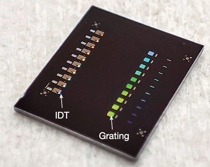
MIT scientists have developed a wafer-scale process to fabricate silicon-photonics chips that are both mechanically flexible and optically transparent, a combination previously unattainable with traditional materials. This scalable technique moves beyond limited lab demonstrations to enable mass production of advanced microchips for emerging applications. “We’ve now developed a wafer-scale process that produces wafers that are mechanically flexible and optically transparent, enabling novel applications that weren’t previously possible with silicon photonics,” says Jelena Notaros, the Robert J. Shillman Career Development Associate Professor of Electrical Engineering and Computer Science at MIT. The new chips could lead to discreet health monitors conforming to the body and transparent augmented-reality displays for pilots. Wafer-Scale Process Enables Flexible, Transparent Silicon Photonics The fabrication process relies on 300-millimeter wafers, a significant increase in scale compared to previous demonstrations limited to fabricating only a few devices at a time. This wafer-scale approach, utilizing existing fabrication tools, allows for mass production and increased confidence in performance metrics, as the team can reliably produce a large number of devices meeting specifications. Achieving both mechanical flexibility and optical transparency simultaneously presented a considerable engineering challenge; traditional silicon photonics chips are rigid and opaque. A key innovation involves a temporary support layer added during fabrication to prevent wafer shattering when flipped, a critical step in creating the flexible structure. Removing this temporary layer leaves only the oxide and waveguiding layers, resulting in a remarkably thin and transparent chip. This process, validated through experimentation, demonstrated performance exceeding the requirements for intended applications. The team’s work confirms the viability of applications benefiting from these unique

Quantum ZeitgeistLoading...0
Giesecke+Devrient Joins European uPQComing Consortium to Develop Quantum-Safe eID Operating Systemsquantum-computing

Giesecke+Devrient Joins European uPQComing Consortium to Develop Quantum-Safe eID Operating Systems

Giesecke+Devrient Joins European uPQComing Consortium to Develop Quantum-Safe eID Operating Systems Munich-based security technology group Giesecke+Devrient (G+D) has joined uPQComing (Enhancing Cyber-Resilience for the Upcoming Post-Quantum Era), a European research consortium co-funded by the European Union’s Chips Joint Undertaking (Chips JU). The project focuses on migrating critical public digital infrastructure and resource-constrained embedded secure elements—specifically smart card integrated circuits and electronic identity (eID) operating systems—to Post-Quantum Cryptography (PQC). [ uPQComing Research Scope & G+D Technical Focus ]Funding & Governance FrameworkHardware & OS Target EnvironmentCryptographic Architecture• EU Chips Joint Undertaking (Chips JU) Co-Funded• Java Card Chip Operating System (OS)• Hybrid Classical/PQC Authentication Protocols• Pan-European Industry & University Consortium• Embedded Secure Elements (eID Smart Cards)• Dynamic Crypto-Agile System Architectures• Focus: Critical Public Digital Infrastructure• Resource-Constrained Memory & Compute Optimization• Terminal-to-Card Secure Communication Channels Embedded PQC Optimization for Java Card Secure Elements Integrating lattice-based post-quantum algorithms into smart card microcontrollers introduces severe performance bottlenecks due to larger key sizes, increased memory consumption, and higher computational overhead compared to classical RSA and ECC. Within uPQComing, G+D is engineering specialized implementation pathways for resource-constrained silicon: Java Card OS Prototyping: Integrating PQC primitives into a native Java Card chip operating system, optimizing instruction execution, RAM usage, and non-volatile memory footprints to maintain rapid authentication times at verification terminals. Crypto-Agile Architecture: Designing flexible firmware layers that allow secure elements to update, swap, or patch cryptographic primitives over time as algorithmic stan

Quantum Computing ReportLoading...0

From Quantum Authors

View Guest Articles

Trending Stories

View All Trending
Quantum News

Get the Quantum News Newsletter

Weekly insights • No spam • Unsubscribe anytime

India National Quantum Mission

Explore India's ₹6,003 Crore quantum initiative: 4 thematic hubs, leading startups, and the latest developments in India's quantum ecosystem

View All India NQM Content