
How Could Integrated Photonics for Atom Trapping Support Practical Quantum Advantage?
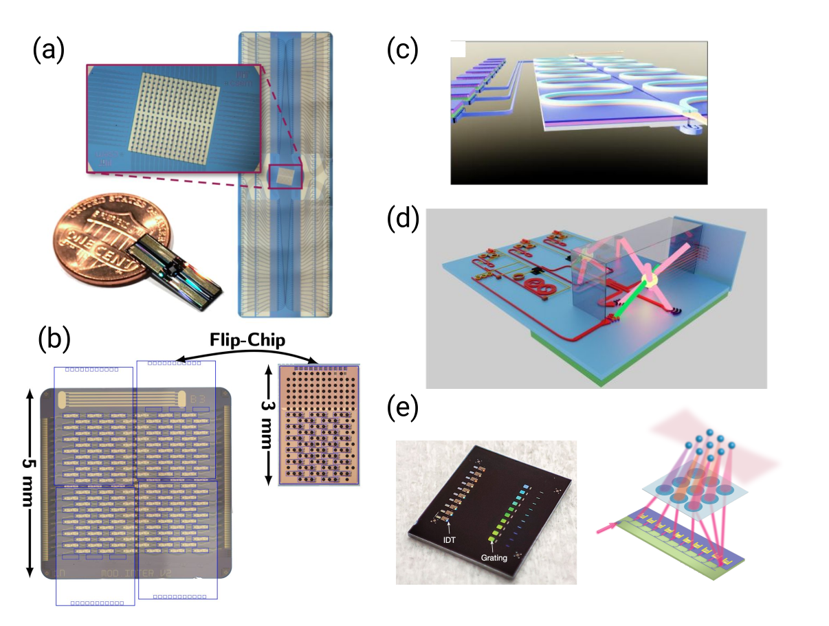
Part 155 of the Neutral Atom Quantum Computation series, covering 3.2.4 Integrated Photonics for Atom Trapping and the roadmap's guidance on integrated photonics for atom trapping.
⚡ Quantum Brief
Trapping optics determine array scale, geometry, transport, and the mechanical stability of the processor. A practical contribution must be demonstrated with complete-system evidence rather than component claims. Track trap depth, beam waist, steering range, update speed, optical efficiency, aberration, crosstalk, and atom lifetime.
Key takeaways
- Integrated trapping systems generate and steer optical potentials from compact photonic devices rather than large free-space assemblies.
- Trapping optics determine array scale, geometry, transport, and the mechanical stability of the processor.
- Devices must handle substantial optical power while preserving beam quality, low loss, fine spatial control, and vacuum compatibility.
- Explore grating emitters, acousto-optic arrays, focal-plane modulators, vertical emitters, and hybrid free-space-chip architectures.
- Track trap depth, beam waist, steering range, update speed, optical efficiency, aberration, crosstalk, and atom lifetime. A meaningful milestone is an integrated device that traps and rearranges a computationally relevant array with stable high-quality sites.
On this page
Short answerWhy it mattersChallenges and constraintsResearch directionsMetrics and milestonesFrequently asked questionsShort answer
Integrated trapping systems generate and steer optical potentials from compact photonic devices rather than large free-space assemblies.
Why it matters
Trapping optics determine array scale, geometry, transport, and the mechanical stability of the processor.
Challenges and constraints
Devices must handle substantial optical power while preserving beam quality, low loss, fine spatial control, and vacuum compatibility.
Research directions
Explore grating emitters, acousto-optic arrays, focal-plane modulators, vertical emitters, and hybrid free-space-chip architectures.
- 1
Integrate the stack
Evaluate the proposal with the control, compilation, and fault-tolerance assumptions needed by a complete processor.
- 2
Measure representative workloads
Prefer repeated circuit and logical-operation evidence over isolated best-case component measurements.
- 3
Make assumptions explicit
Report scale, error model, calibration, classical support, and resource-accounting boundaries.
Metrics and milestones
Track trap depth, beam waist, steering range, update speed, optical efficiency, aberration, crosstalk, and atom lifetime.
A meaningful milestone is an integrated device that traps and rearranges a computationally relevant array with stable high-quality sites.
| Dimension | What to report | Why it matters |
|---|---|---|
| Component performance | Track trap depth, beam waist, steering range, update speed, optical efficiency, aberration, crosstalk, and atom lifetime. | Shows whether the underlying mechanism is improving. |
| System performance | Behavior in a representative circuit or repeated operating cycle. | Reveals integration overhead and correlated failures. |
| Strategic milestone | A meaningful milestone is an integrated device that traps and rearranges a computationally relevant array with stable high-quality sites. | Connects laboratory progress to useful neutral atom computation. |
Frequently asked questions
What is the central goal of integrated photonics for atom trapping?
Integrated trapping systems generate and steer optical potentials from compact photonic devices rather than large free-space assemblies.
Why is integrated photonics for atom trapping strategically important?
Trapping optics determine array scale, geometry, transport, and the mechanical stability of the processor.
What is the main obstacle for integrated photonics for atom trapping?
Devices must handle substantial optical power while preserving beam quality, low loss, fine spatial control, and vacuum compatibility.
What research does the strategic plan recommend for integrated photonics for atom trapping?
Explore grating emitters, acousto-optic arrays, focal-plane modulators, vertical emitters, and hybrid free-space-chip architectures.
What would count as convincing progress in integrated photonics for atom trapping?
Track trap depth, beam waist, steering range, update speed, optical efficiency, aberration, crosstalk, and atom lifetime. A meaningful milestone is an integrated device that traps and rearranges a computationally relevant array with stable high-quality sites.
Related answers
Methodology
This editorial draft is a structured transformation of Strategic Plan for Neutral Atom Quantum Computation (arXiv:2607.21554), especially 3.2.4 Integrated Photonics for Atom Trapping, pages 46-48. Claims are summarized rather than copied at length. The article remains a draft until a technical reviewer checks the interpretation, figure context, and any developments published after 23 July 2026.
Update history
24 July 2026 — Initial source-grounded draft generated for the Neutral Atom Quantum Computation Answers series.
Corrections
Found an error or newer technical evidence? Contact the QuantumNews editorial team.
References
Discussion
0 professional contributions
Sign in to join this professional discussion.
Be the first to add a constructive contribution.