QuantaMap Breakthrough Published in ACS Nano Letters Accelerates Quantum Materials Research
Understand this faster with AI
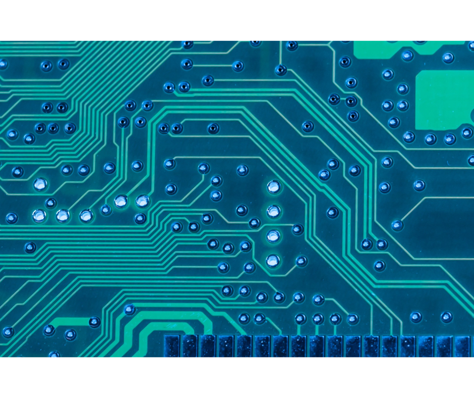
Dutch quantum technology startup QuantaMap and Leiden University have unveiled a revolutionary microscope capable of simultaneously imaging heat, magnetism, structure, and electrical behavior at the nanoscale, published today in ACS Nano Letters. This breakthrough addresses a critical bottleneck in quantum chip development – understanding localized behavior within real-world devices, moving characterization beyond idealized lab conditions. The new multi-modal imaging platform allows researchers to probe interacting physical phenomena with unprecedented resolution without disturbing the chip itself. “In a real quantum device, all physical properties are closely intertwined. If you only study one aspect at a time, you never get ahead,” explains lead author Matthijs Rog of Leiden University. This technology promises to accelerate design optimization, increase fabrication yield, and ultimately, enable scalable quantum manufacturing. Multi-Modal Nanoscale Imaging Reveals Quantum Chip Behavior Published in Nano Letters on February 12, 2026, the new platform addresses a key challenge in scaling quantum technologies – understanding localized chip behavior in real-world devices. Unlike conventional testing which can take weeks per chip, this technology allows for nanoscale root-cause analysis at any fabrication stage, correlating performance with local material properties. “Current chip testing relies mainly on electrical characterization of fully finished chips inside quantum computers – a process that takes weeks per chip and if the performance of some qubits is reduced, it cannot reveal the underlying reason,” says Johannes Jobst, founder and CEO of QuantaMap. The microscope achieves this by employing tapping mode feedback for stable, extended measurements on realistic, nanostructured devices—including functioning quantum chips and novel quantum materials. Researchers can now probe multiple interacting physical phenomena at once, without disturbing the chip itself. “With our microscope, we reveal the relationships between non-equilibrium properties such as current and dissipation, and how those relate to chip structure.” This capability promises to boost fabrication yield and accelerate design optimization. Root-Cause Failure Analysis Accelerates Quantum Fabrication This limitation hinders progress toward scalable quantum manufacturing, as identifying the root cause of qubit degradation remains a significant challenge. QuantaMap, in collaboration with Leiden University, is now offering a solution with a new nanoscale imaging platform designed to move characterization beyond idealized lab conditions and directly onto operational quantum chips. The technology promises to correlate device performance with local material behavior, enabling faster iteration between design, fabrication, and testing. The platform’s stability, achieved through tapping mode feedback, allows for extended measurement campaigns on realistic, nanostructured devices, ultimately increasing fabrication yield and consistency, according to QuantaMap. The ability to perform root‑cause analysis at the nanoscale makes it possible to identify reasons for failure in quantum chips at any fabrication stage, correlating device performance with local material behavior, and faster design-fabrication-test feedback loops.Johannes Jobst, Founder and CEO of QuantaMap Source: https://pubs.acs.org/doi/10.1021/acs.nanolett.5c04571 Tags: Quantum News As the Official Quantum Dog (or hound) by role is to dig out the latest nuggets of quantum goodness. There is so much happening right now in the field of technology, whether AI or the march of robots. But Quantum occupies a special space. Quite literally a special space. A Hilbert space infact, haha! Here I try to provide some of the news that might be considered breaking news in the Quantum Computing space. Latest Posts by Quantum News: Protected: Quantum Innovation Summit 2026 to Focus on Quantum Readiness & Deployment February 12, 2026 QuTech Demonstrates Key Parity Readout for Majorana Qubits February 12, 2026 Lawrence Berkeley National Lab Unveils Robotic System to Accelerate Qubit Development February 11, 2026
Tags
Source Information
Discussion
0 professional contributions
Sign in to join this professional discussion.
Be the first to add a constructive contribution.