D-Wave Outlines Superconducting Gate-Model Roadmap Targeting 100 Logical Qubits
Understand this faster with AI
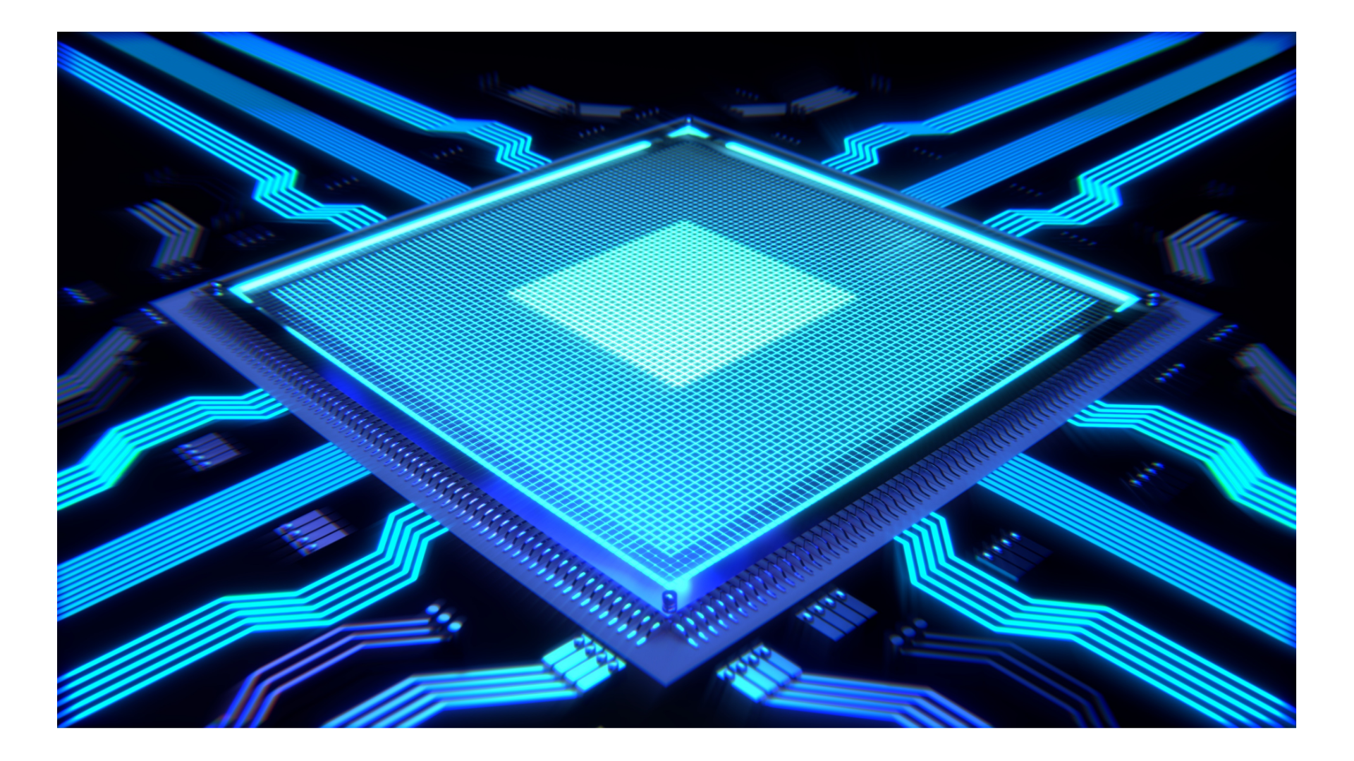
D-Wave Outlines Superconducting Gate-Model Roadmap Targeting 100 Logical Qubits D-Wave Quantum Inc. (NYSE: QBTS) has unveiled a gate-model development roadmap aimed at the production of commercial, fault-tolerant quantum computing systems. Announced at the firm’s inaugural Investor Day at the New York Stock Exchange, the strategic plan outlines a trajectory to deliver a 100-logical-qubit system capable of executing over one million operations by 2032. This long-term system architecture incorporates the asset portfolio of recent acquisition Quantum Circuits, Inc., combining D-Wave’s existing cryogenic infrastructure with a specialized superconducting dual-rail qubit design and integrated quantum error correction (QEC). Technical Architecture & Dual-Rail Qubit Error Detection The technical roadmap focuses on hardware-level error reduction to decrease the physical qubit overhead typically required for error correction. While standard superconducting transmon architectures cannot inherently identify errors during active gate cycles, D-Wave’s superconducting dual-rail architecture embeds error-detection mechanisms directly into the individual qubit components. This hardware-level layout is engineered to identify approximately 90% of physical errors as they occur during computation. By isolating errors at the single-qubit level, the dual-rail system has demonstrated a baseline 99.9% two-qubit gate fidelity across early testing configurations. A core metric guiding D-Wave’s scaling framework is Lambda (λ), which measures the rate of error reduction achieved per increment of added error-correction capability. While contemporary multi-qubit platforms operate at a Lambda value of approximately 2—halving errors with each correction step—D-Wave’s roadmap targets a Lambda value of 10. This error-suppression metric leverages the fast cycle times of superconducting circuits, which execute error correction routines 100 to 1,000 times faster than neutral-atom or trapped-ion alternatives. The phased development timeline schedules a 17-physical-qubit system in 2026 to achieve a 2x logical error reduction, scaling to a 49-physical-qubit array in 2027 (20x error reduction), and a 181-physical-qubit architecture in 2028 to establish a 2,000-fold error suppression blueprint. Enterprise Integration & Dual-Platform Positioning The execution of this gate-model roadmap establishes D-Wave as a dual-platform hardware provider, supplementing its established line of commercial quantum annealing systems, such as the Advantage2™ processor. The completed gate-model chips will be integrated directly into the company’s existing Leap™ quantum cloud service infrastructure, allowing enterprise users to run hybrid classical-quantum workflows. By targeting a 10-logical-qubit array by 2030 to execute early fault-tolerant algorithms, followed by the 100-logical-qubit tier by 2032, the platform is designed to offload dense matrix calculations for quantum artificial intelligence and molecular chemistry simulations, positioning the hardware to address optimization and gate-model workloads simultaneously. You can review the official corporate strategy release via the D-Wave Quantum newsroom here. Learn more about D-Wave’s gate-model roadmap and technology here. June 1, 2026 Mohamed Abdel-Kareem2026-06-01T07:50:41-07:00 Leave A Comment Cancel replyComment Type in the text displayed above Δ This site uses Akismet to reduce spam. Learn how your comment data is processed.
Tags
Source Information
Discussion
0 professional contributions
Sign in to join this professional discussion.
Be the first to add a constructive contribution.