Wafer-Scale Manufacturing Unlocks Path to Quantum Computers with Millions of Qubits
Summarize this article with:
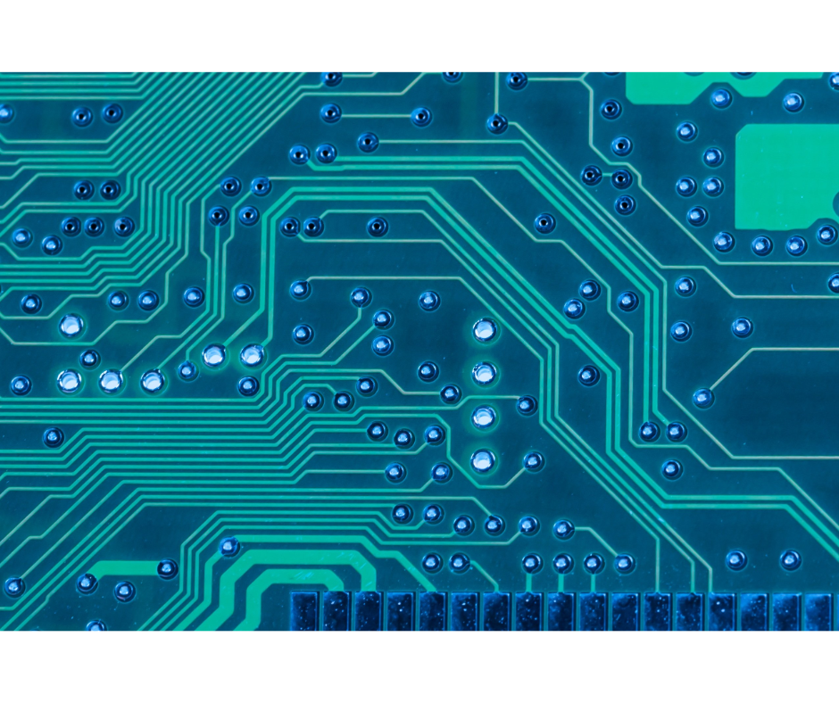
A complete design and manufacturing pipeline for wafer-scale chips now exists, addressing a key hurdle in scaling up superconducting quantum computers. Ling Qiao and colleagues at USTC present a systematic approach to electronic design automation (Q-EDA) that bridges the gap between quantum circuit design and actual chip fabrication. The research converts design layouts into manufacturing-ready files, enabling larger, more cost-effective quantum processors with potentially thousands of qubits. By analysing key stages, from design rule checking to mask data preparation, and benchmarking existing tools, the team highlights current capabilities and essential future developments in wafer-scale quantum manufacturing. Wafer-scale fabrication and design rule optimisation of high-coherence superconducting qubits Superconducting transmon qubits, now fabricated on a 300mm CMOS production line, exhibit relaxation and coherence times exceeding 100μs. This represents a substantial improvement over previous iterations, which were limited to proof-of-concept stages and suffered from significantly shorter coherence times, typically in the microsecond range. This milestone signifies a transition from experimental devices to engineered systems capable of supporting complex quantum computations, opening avenues for exploring more intricate quantum algorithms and error correction schemes. Researchers of Technology and imec detailed a systematic quantum-chip electronic design automation (Q-EDA) technology stack for wafer-scale fabrication, focusing on converting GDSII files, the standard format for chip designs, into manufacturing-ready instructions. The move to 300mm wafers is particularly significant, as it leverages existing, high-volume CMOS infrastructure, reducing fabrication costs and increasing potential throughput compared to smaller wafer sizes. The system incorporates nine quantum-specific design rule checks, addressing unique challenges in superconducting circuit fabrication, such as maintaining microwave signal integrity and minimising qubit decoherence. These challenges stem from the extreme sensitivity of superconducting circuits to electromagnetic noise and imperfections in the fabrication process. It utilises a single authoritative data source, GDSII files, to avoid data inconsistencies common in multi-tool workflows, and encodes process rules in structured JSON, allowing rapid adaptation to different fabrication facilities. This centralised data management is crucial for ensuring design integrity and traceability throughout the manufacturing process. Furthermore, the system unifies physical verification, design for manufacturability optimisation, and mask data preparation into a single automated pipeline, streamlining the process and reducing potential errors. These checks include enforcing a minimum coplanar waveguide gap of 3μm to control two-level system losses, which arise from unwanted spurious modes in the microwave transmission lines, and ensuring Josephson junction overlap tolerances of ±50nm for critical current control. Precise control of the Josephson junction parameters is vital for achieving consistent qubit performance. The stack is capable of completing 76 geometric rule checks on a test chip containing 28 parameterised components in just 0.23 milliseconds, demonstrating its efficiency and scalability for complex designs. This speed is essential for iterative design optimisation and rapid prototyping. Quantum circuit layout verification using automated layout-versus-schematic comparison Layout-versus-schematic (LVS) verification underpins the entire data conversion process, acting as an important safeguard against errors. This technique carefully compares the physical layout, the blueprint for a microchip, with its original electrical schematic. It confirms that the intended circuit functions are accurately represented in the physical design, much like verifying a wiring diagram against the actual wiring in a circuit. Implementing LVS for quantum circuits is particularly challenging due to the complex, multi-layered superconducting structures and the need to account for quantum-specific parameters, but it is essential for identifying discrepancies before fabrication. Traditional LVS tools are designed for conventional semiconductor devices and require significant adaptation to handle the unique characteristics of superconducting qubits, such as the absence of active transistors and the reliance on Josephson junctions. Automated comparison ensures designs are not only electrically correct but also physically realisable, minimising costly errors and maximising yield in wafer-scale manufacturing. The architecture comprises four layers: project management, design capture, verification and process mapping, and tape-out and foundry export. Data flows sequentially through these layers from initial design to manufacturing files. This layered approach facilitates efficient error detection and correction throughout the fabrication process. The project management layer handles version control and design data management, while the design capture layer translates the quantum circuit description into a physical layout. The verification and process mapping layer performs LVS and design rule checking, ensuring the design meets all fabrication requirements. Finally, the tape-out and foundry export layer generates the manufacturing files needed by the fabrication facility. Adapting semiconductor design automation for scalable quantum processor manufacture Wafer-scale fabrication offers a clear path towards building quantum computers with the thousands of qubits needed for practical applications, yet translating designs into physical chips remains a complex undertaking. Acknowledging limitations in fully benchmarking against dedicated quantum tools is sensible, and a detailed mapping of existing semiconductor design processes onto quantum-chip fabrication is a vital step forward. Wafer-scale fabrication, creating many qubits on a single chip, demands strong design automation, and adapting established techniques provides a key foundation. The development of dedicated Q-EDA tools is ongoing, but leveraging the maturity and robustness of existing semiconductor tools provides a pragmatic approach for accelerating progress. Progress is accelerated by identifying specific design rule checks and data conversion stages, even as custom quantum tools mature and become more readily available. Establishing a systematic quantum-chip electronic design automation stack is now key for translating designs into wafers suitable for large-scale fabrication. This work details an architecture utilising GDSII files as a central data source, streamlining conversion into manufacturing instructions; it moves beyond simply designing individual quantum bits to focus on complete fabrication workflows. The fabrication of a significant number of qubits, such as the 504 qubits achieved, will begin a new era in quantum computing, paving the way for more complex and powerful quantum processors. Achieving fault-tolerant quantum computation will require millions of physical qubits, and wafer-scale fabrication, coupled with robust Q-EDA tools, is essential for reaching this goal. Further research will focus on optimising the design rules for specific qubit architectures and developing automated techniques for calibrating and characterising large-scale quantum processors. The researchers successfully detailed a systematic approach to electronic design automation for wafer-scale quantum chip fabrication. This is important because building larger quantum computers with thousands of qubits requires a reliable method for translating designs into physical chips efficiently and accurately. The work establishes a complete data-conversion pipeline, starting with GDSII files, and identifies nine quantum-specific design rule checks. Future research will concentrate on refining these design rules and automating the calibration of large quantum processors, building on the foundation of 504 qubits already achieved. 👉 More information🗞 From GDSII to Wafer: EDA Design Flow and Data Conversion for Wafer-Scale Manufacturing of Superconducting Quantum Chips🧠 ArXiv: https://arxiv.org/abs/2604.11379 Tags: