Harvard Breakthrough Brings Powerful UV Light Sources Onto a Chip
Summarize this article with:
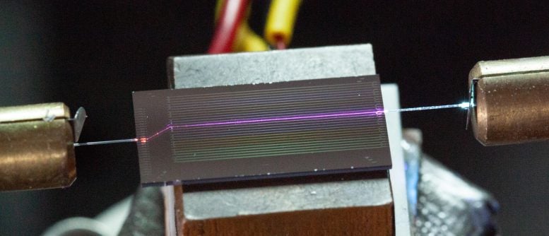
Camera image of the sidewall-poled lithium niobate chip during UV generation. Credit: Loncar Lab / Harvard SEASScientists have achieved a major step toward chip-scale ultraviolet light by converting red light into powerful UV within a tiny photonic device.Ultraviolet light, beyond what comes naturally from the sun, plays a central role in modern technology, including sterilization, biological imaging, and chip manufacturing. Researchers also expect tiny sources of UV light on photonic chips to support future advances in quantum computing and ultra-precise atomic clocks.However, shrinking UV light sources to the chip scale has proven difficult because this light quickly loses strength as it travels through optical waveguides, limiting practical designs until now.A Harvard-led team from the lab of Marko Lončar, the Tiantsai Lin Professor of Electrical Engineering, has demonstrated a micron-scale photonic device built on thin-film lithium niobate that produces about 100 times more UV light on a chip than earlier methods. The study, published in Nature Communications, highlights lithium niobate as a promising platform for compact, efficient, and high-power UV generation.Instead of trying to directly guide UV light, the device generates it internally by converting red light into UV. This process, called frequency upconversion, combines two red photons inside the lithium niobate crystal, which is highly efficient at frequency conversion, to produce a single higher-energy UV photon.“Our group is perhaps best known for utilizing lithium niobate for photonic devices that operate at longer, infrared wavelengths – closer to the realm of telecommunications signals,” Lončar said. But he added that this transparent crystalline material, already widely used in integrated photonics, can also guide and generate shorter wavelengths such as UV.“When people think about [thin-film lithium niobate], they don’t think of it as a UV material, but we show that it is,” said co-first author Kees Franken, former research fellow in the Lončar lab. “We also show that there are some other nonlinear effects happening that we don’t fully understand yet.”New method: Sidewall polingInside the device, light travels through waveguides, which are microscopic channels etched into the material. Efficiently converting red light into UV requires carefully flipping the crystal structure at regular intervals along the waveguide, a nanofabrication process known as poling. Achieving this precise pattern at submicron scales over centimeter-length (about 0.4 inch) devices has been a major obstacle.Earlier methods involved tradeoffs. Poling the entire film reduced flexibility to correct fabrication flaws, while forming the waveguides first limited efficiency because electrodes were too far away and only partially influenced the material.Scanning electron microscope image of metal electrodes used for sidewall poling. Credit: Loncar Lab / Harvard SEASThe team addressed this challenge with a technique called “sidewall poling.”Rather than placing electrodes only on top of the film, they positioned finely patterned metal “fingers” directly along the sides of the waveguide. A small voltage applied during fabrication flips the crystal domains in a tightly controlled arrangement.“The key idea was: could we just put the electrodes directly on the waveguide?” said co-first author and former graduate student Soumya Ghosh. “It’s a high-precision fabrication process to position the electrodes but requiring about 50-nanometer accuracy.”This approach ensures the crystal is fully inverted across the entire waveguide cross section, allowing the light to interact with an optimally structured material and maximizing conversion efficiency. The researchers also adjusted the spacing of the flipped regions along the device using “adapted poling” methods developed in the Lončar lab and elsewhere to compensate for variations in thickness and shape.Results show increased power outputThe team reports 4.2 milliwatts of on-chip UV light at a wavelength of 390 nanometers, which is about 120 times higher than previous thin-film lithium niobate devices operating in this range. Earlier efforts produced only tens of microwatts, enough to demonstrate the concept but not sufficient for practical use.Reliable chip-scale UV light sources are important for emerging systems such as trapped-ion quantum computers, where key atomic transitions occur in the near UV.“If you want a scalable quantum computer that isn’t the size of a truck, you need to scale everything down to the chip level, and this includes the light sources,” Franken said.The same wavelength range could also support compact environmental sensors for tracking greenhouse gases and other air pollutants.Franken and Ghosh said the progress reflects the group’s ability to handle every stage of development in-house, from theory and design to fabrication and testing.“The hands-on intuition that we gained for how to make a device, while also keeping the zoomed-out view of what this device is for, and how we were going to characterize it – that’s a big part of what enabled this project for us,” Ghosh said.Reference: “Milliwatt-level UV generation using sidewall poled lithium niobate” by C. A. A. Franken, S. S. Ghosh, C. C. Rodrigues, J. Yang, C. J. Xin, S. Lu, D. Witt, G. Joe, G. S. Wiederhecker, K.-J. Boller and M. Lončar, 21 April 2026, Nature Communications. DOI: 10.1038/s41467-026-68524-yFunding: Department of the Air Force grant No. FA9453-23-C-A039; Office of Naval Research grant No. N00014-22-C-1041/VAS-21-0001; NASA grant No. 80NSSC22K0262 and 80NSSC23PB442; and National Science Foundation grants ERC EEC-1941583 and OMA-2137723.Never miss a breakthrough: Join the SciTechDaily newsletter.Follow us on Google and Google News.